- Published 31 Mar 2023
- Last Modified 29 Aug 2023
- 6 min
A Complete Guide to IGBTs
Our guide sets out everything you need to know about IGBTs, including applications, how they work, and FAQs.

Published December 2021. Last Updated January 2022
MOSFETs and bipolar junction transistors (BJTs) are among the most common electronic power switching devices. However, both components have limitations - particularly when used in high current applications. IGBTs are an alternative type of device combining the benefits and characteristics of both a BJT and a MOSFET.
But what is an IGBT and how do they work? In this guide, we will explore insulated gate bipolar transistors, covering their applications, types, and how they differ from other devices.
What is an IGBT?
An insulated gate bipolar transistor (IGBT) is a type of discrete semiconductor that essentially combines features from both MOSFETs and bipolar transistors. These power modules incorporate the high voltage and current handling capabilities of bipolar transistors alongside the high-speed switching performance of power MOSFETs. In other words, IGBTs can handle large collector-emitter currents with very low gate current drive.
IGBT modules have three terminals and consist of four alternating layers, controlled by a metal-oxide-semiconductor gate structure. They are also unidirectional, meaning that they are only able to switch current in the forward direction. This differs from MOSFETs which have the capacity for bi-directional current switching.
What are IGBTs Used for?
As these modules combine the benefits of both BJTs and MOSFETs, they are often used in power supply and motor control circuits. They are frequently found in power electronics applications where the demands cannot be met by power MOSFETs and transistors alone.
Similarly, IGBT modules are also typically used as electronic switching devices. This is because they combine fast switching with high efficiency, making them ideally suited to this task. When being used as a static controlled switch, IGBTs have current and voltage ratings akin to those of a bipolar transistor. However, the presence of the isolated gate gives them the advantage as much less drive power is required.

Standard IGBT applications are high-voltage and moderate speed. They could include:
- Variable speed control
- Switch-mode power supplies (SMPS)
- DC-AC inverters
- Driving inductive loads
- Pulse-width modulation (PWM)
- AC and DC motor drives
- Frequency converters
- Traction motor control
How Does an IGBT Work?
As the name suggests, insulated gate bipolar transistors combine technology from both MOSFETs and bipolar junction transistors.
The first part of the name refers to the insulated gate, like a MOSFET, while the second part references the output performance characteristics of a standard bipolar transistor. This shows that IGBT devices are voltage controlled like MOSFETs while maintaining the conduction characteristics and output switching of transistors. In a nutshell, IGBTs offer greater power gain than BJTs and higher voltage operation with lower input losses than a MOSFET. They combine a PNP transistor output with an insulated gate N-channel MOSFET output.
IGBTs are transconductance modules with three terminals. These terminals are the emitter, collector, and gate. The latter controls the device while the first two are linked to the current and the conductance path.
As is the case with a power BJT, the amplification amount is determined by a ratio between the input and output signals. However, as the gate is isolated from the current-carrying channel in an IGBT, there is no input current. Therefore, the base current is provided by a MOSFET.
IGBT Construction
IGBT modules are formed from four layers of semiconductors that are sandwiched together. These are:
- P+ substrate layer (closest to the collector terminal)
- N- layer
- P layer (closest to the emitter terminal)
- N+ layer (within the P layer, but not present in all devices)
IGBT Types
IGBT transistors can be classified in two ways. This is based on the N+ buffer layer, which as explained above, is one of the layers of semiconductor present inside the P layer. Those devices that have this layer are known as punch-through IGBTs, whereas those that don't are referred to as non-punch-through IGBTs.
They may also be called symmetrical and non-symmetrical IGBTs based on these characteristics. Symmetrical devices have equal forward and reverse breakdown voltage whereas those that are non-symmetrical have reverse breakdown voltage that is less than the forward breakdown voltage. This is why non-symmetrical IGBTs are typically used in DC circuits since there isn't a requirement to support voltage in the reverse direction.
Package & Mounting Type
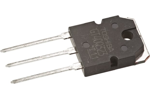
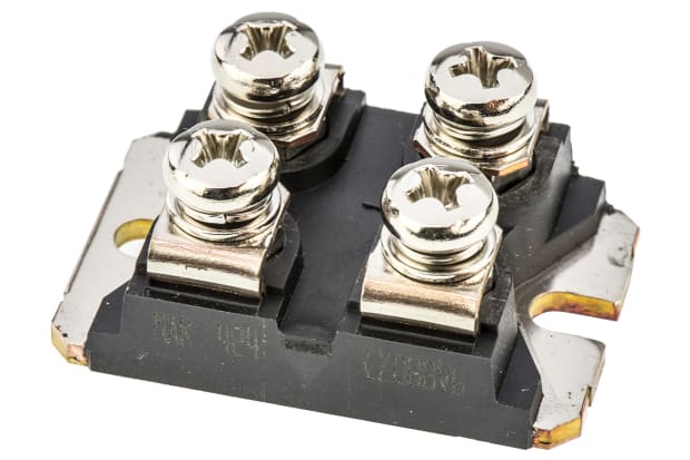
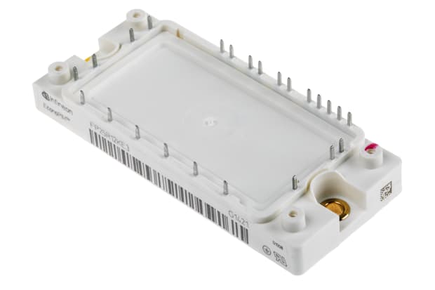
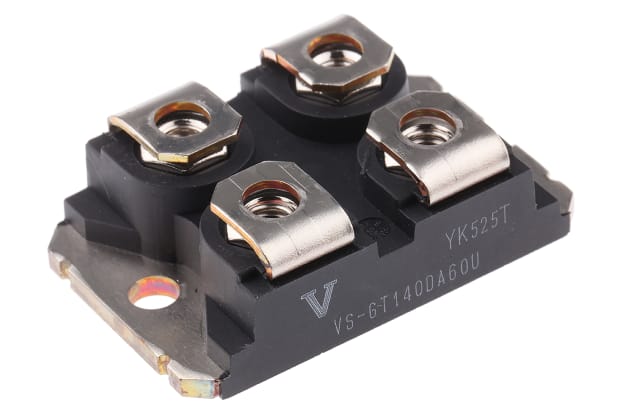
There are various package IGBTs available depending on the particular manufacturer. This will also depend on the mounting type - for example, through-hole, panel-mount, or surface-mount.
Popular brands and manufacturers include:
FAQs
What are the Advantages of IGBTs?
Due to their hybrid configuration, there are many advantages to using IGBT modules over other types of power transistors. Advantages include:
- High voltage capabilities
- Simplicity of drive
- Low on-state power dissipation
- Low resistance
- Fast switching speed
What is the Difference Between IGBT vs MOSFET?
Although MOSFETs and IGBTs are similar components, both transistors also have key differences. A few of the primary differences between IGBTs and MOSFETs are outlined below.
IGBT power modules are preferred for high voltage applications as they are constructed specifically to perform under high voltage. To put that into context, IGBTs have a typical voltage rating of around 1400V while MOSFETs are much lower rated at around 600V.
The two device types also have different terminals despite their similar structure, with the three terminals of an IGBT (emitter, collector, gate) differing from those of a MOSFET (source, drain, gate).
You can see a comparison between the two device types in this table:

How Do I Control IGBTs?
IGBT transistors can be turned on or off by either activating or deactivating the gate terminal. For the on state, a positive input voltage must be applied across the gate, signalling the emitter to keep the device on. Since these devices are voltage controlled, only a small voltage on the gate is needed to maintain conduction through the IGBT module. For the off state, changing the input gate to receive a zero or negative signal will trigger the device to turn off.
How Do You Test IGBTs?
IGBT testing is important to ensure the device and diodes are in good condition. Testing can also identify if the gate terminals are properly insulated.
IGBT modules can be easily tested with a multimeter however if more comprehensive circuit diagnostics are required, it is always recommended to consult an expert. You should also bear in mind that these modules can be highly sensitive to ESD so anti-static protective equipment should always be used when handling IGBT transistors.


