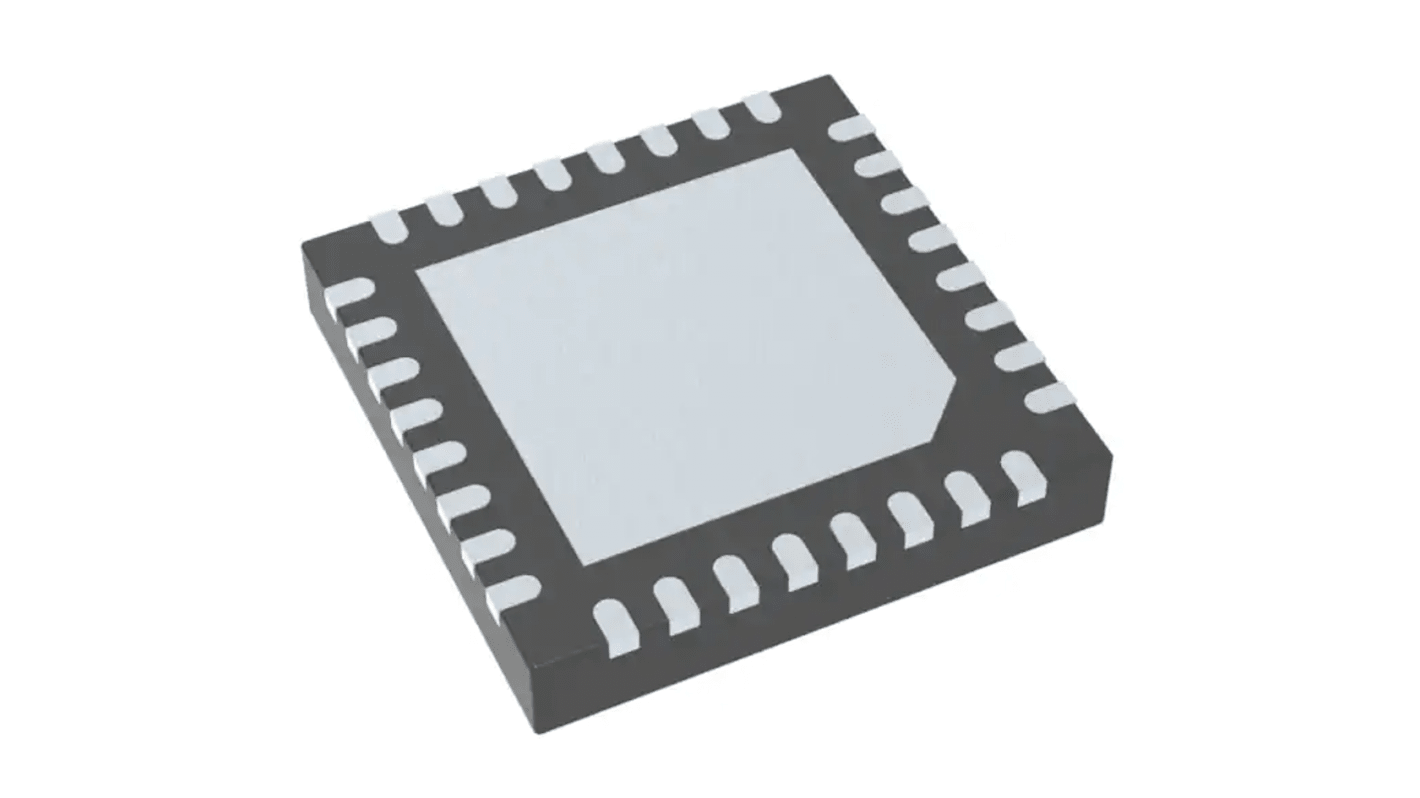
Renesas Electronics 9DML4493ANLGI Clock Buffer 32-Pin VFQFPN
- RS Stock No.:
- 264-1310
- Mfr. Part No.:
- 9DML4493ANLGI
- Manufacturer:
- Renesas Electronics

Subtotal (1 tray of 490 units)*
€2,333.87
(exc. VAT)
€2,870.42
(inc. VAT)
Temporarily out of stock
- Shipping from 26 March 2027
Need more? Click ‘Check delivery dates’ to find extra stock and lead times.
Units | Per unit | Per Tray* |
|---|---|---|
| 490 + | €4.763 | €2,333.87 |
*price indicative
- RS Stock No.:
- 264-1310
- Mfr. Part No.:
- 9DML4493ANLGI
- Manufacturer:
- Renesas Electronics
Specifications
Technical data sheets
Legislation and Compliance
Product Details
Find similar products by selecting one or more attributes.
Select all | Attribute | Value |
|---|---|---|
| Brand | Renesas Electronics | |
| Product Type | Clock Buffer | |
| Maximum Input Frequency | 350MHz | |
| Mount Type | Surface | |
| Maximum Propagation Delay Time | 1.2ns | |
| Package Type | VFQFPN | |
| Pin Count | 32 | |
| Minimum Supply Voltage | 1.8V | |
| Maximum Supply Voltage | 3.63V | |
| Minimum Operating Temperature | -40°C | |
| Maximum Operating Temperature | 85°C | |
| Series | 9DML4493A | |
| Standards/Approvals | RoHS | |
| Length | 5mm | |
| Height | 1mm | |
| Automotive Standard | No | |
| Select all | ||
|---|---|---|
Brand Renesas Electronics | ||
Product Type Clock Buffer | ||
Maximum Input Frequency 350MHz | ||
Mount Type Surface | ||
Maximum Propagation Delay Time 1.2ns | ||
Package Type VFQFPN | ||
Pin Count 32 | ||
Minimum Supply Voltage 1.8V | ||
Maximum Supply Voltage 3.63V | ||
Minimum Operating Temperature -40°C | ||
Maximum Operating Temperature 85°C | ||
Series 9DML4493A | ||
Standards/Approvals RoHS | ||
Length 5mm | ||
Height 1mm | ||
Automotive Standard No | ||
- COO (Country of Origin):
- TW
The Renesas Electronics 4-input, 4-output clock multiplexer. It can also operate as a dual 2-input, 2-output clock multiplexer. It has very low additive phase jitter and is suitable for all PCIe data rates. The device supports todays complex system power sequencing requirements with Power Down Tolerant and Flexible Power Sequencing features.
Supports common Clocked (CC) and IR (SRIS, SRNS) timing architectures
Glitch-free output enable pins for each output
Spread-spectrum tolerant
Related links
- Renesas Electronics 9DML4493ANLGI Clock Buffer 32-Pin VFQFPN
- Renesas Electronics 9DBV0441AKLF Clock Buffer 32-Pin VFQFPN
- Renesas Electronics 9DBV0441AKILF Buffer 32-Pin VFQFPN
- onsemi NB7L572MNG PLL Clock Buffer 32-Pin QFN
- onsemi PLL Clock Buffer 32-Pin QFN
- Renesas Electronics Clock Buffer 16-Pin VFQFPN
- Renesas Electronics 5PB1216NDGK Clock Buffer 20-Pin VFQFPN
- Renesas Electronics 9DBV0831AKILF Clock Buffer 48-Pin VFQFPN