- Automation & Control Gear
- Cables & Wires
- Enclosures & Server Racks
- Fuses & Circuit Breakers
- HVAC, Fans & Thermal Management
- Lighting
- Relays & Signal Conditioning
- Switches
- Batteries & Chargers
- Connectors
- Displays & Optoelectronics
- ESD Control, Cleanroom & PCB Prototyping
- Passive Components
- Power Supplies & Transformers
- Raspberry Pi, Arduino, ROCK, STEM Education & Development Tools
- Semiconductors
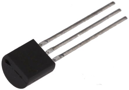
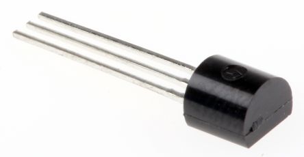
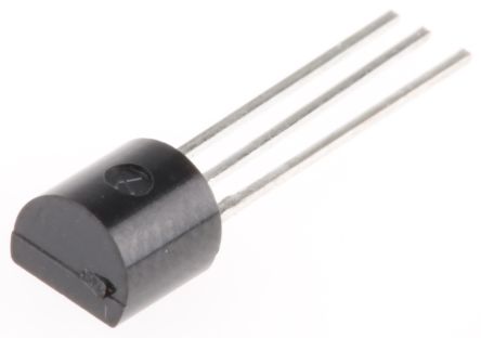
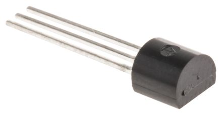
JFETs
A JFET is a four-terminal device, the terminals are called the gate, drain, source and body. The body terminal is always connected to the source. There are two types of JFETs and N-Channel P-Channel. FET stands for junction field-effect transistor. They can also be referred to as a JUGFET
N-Channel JFET Construction
The name N-Channel signifies that the electrons are the majority charge carriers. To form the N-Channel an N type semiconductor is used as a base and doped with a P type semiconductor at both ends. Both these P regions are electrically linked together with an ohmic contact at the gate. Two further terminals are taken out at the opposite ends for the drain and the source.
P-Channel JFET Construction
The name P channel signifies that the holes are the majority charge carriers. To form the P-Channel a P type semiconductor is used as a base and doped with an N type semiconductor at both ends. Both these N regions are electrically linked together with an ohmic contact at the gate. Two further terminals are taken out at the opposite ends for the drain and the source.
Features and Benefits
- High input impedance
- Voltage-controlled device
- A high degree of isolation between the input and the output
- Less noise
What are JFET transistors used for?
JFET transistors have many applications in electronics and communication. You can use them as an electronically controlled switch to control electric power to a load, and as amplifiers.
What is the difference between a JFET and BJT (Bipolar Junction Transistor)?
The main difference between a JFET and BJT is a field effect transistor only majority charge carrier flows while the BJT (bipolar transistor) offers both majority and minority charge carriers flow.
What is the doping of semiconductors?
Doping is the process of including foreign impurities to intrinsic semiconductors to change their electrical properties. Trivalent atoms used to dope silicon cause an intrinsic semiconductor to become a P-Type semiconductor. Pentavalent used to dope silicon cause an intrinsic semiconductor to become an N-Type semiconductor.